
(b) When U120 receives the write command, the device samples the
incoming analog signal (pin 6) and begins its (digital) conversion internally.
(c) After the conversion is complete, the device outputs the signal's
digital value on pins 11 through 18 and momentarily asserts pin 5 low. When the pulse at
U120 pin 5 returns high, U121 latches and holds the digital value presented to it by U120
pins 11 through 18.
(d) When U121 pin 1 receives a low pulse from U127 pin 16, U121
enables its output pins. This makes its internally latched data available Lo random access
memory (RAM) U124. The pulse seen at U127 pin 16 is an inversion of the pulse seen at
U127 pin 9.
(4)
Memory.
(a) The data storage device for this system is U124. U124 is a CMOS
2K x 8 RAM. Digitized analog data from the A/D converter (U120) is stored in this device
during a RAM write cycle. Data stored in this device is output on its data pins (pins 9
through 11, 13 through 1) during a RAM rad cycle.
(b) U124 is normally held in a RAM read cycle mode. This mode is
characterized by U124 pin 20 being low and U124 pin 21 being high. When U123 pin 16
(retrace blanking) is high, the RAM is outputting data.
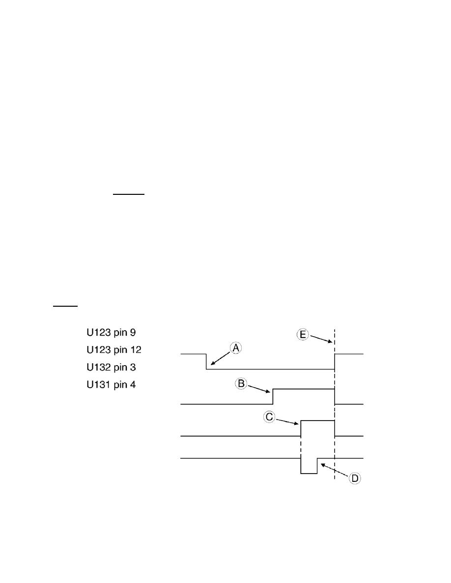
NOTE:
Refer to figure 2-1 for an illustration related to paragraphs (c) through (f).
Figure 2-1. Timing diagram.
MD0362
2-20

 Previous Page
